Ultrasonic Theremin - Junior Design
Date: 11/2022
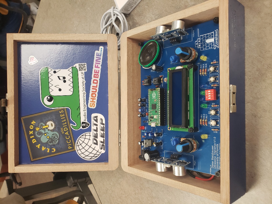
Ultrasonic Theremin in its case.
Introduction
The Theremin is a musical instrument designed by Leon Theremin in 1928. The device operates using two antennas relying on capacitor physics, which sense the position of the operator’s hands. One antenna influences the output frequency of the note, while the other influences the volume of the note. While the original theremin operates on a series of analog systems, I intend to implement similar systems in the digital domain by using the ultrasonic sensors to determine distance between the instrument and the operator’s hands. The digital and analog inputs will augment a waveform generator, which creates an audio signal according to the user’s movements, creating a digital instrument.
Methods
Project Overview
The raspberry Pico interfaces with multiple components and generates waveform functions for audio output. Ultrasonic sensors detect distance from the users’ hands for frequency determination. Status of the device is displayed on an LCD. Switches and Buttons are available on the device for interaction, selecting output waveforms and other menu options. Potentiometers are connected to the Pico ADC for controlling the upper and lower boundaries of the frequency range. LED’s will assist by lighting up when a boundary is hit.
All generated waveforms are sent to the DAC via SPI and then to the LM386 audio amplifier, which drives the 8-ohm speaker. Everything can be powered using a 9V battery or adapter, as 5V is generated using the LM2940 LDO. This powers most standalone components, including the Pico. The SMPS on the Pico also generates 3.3V and is filtered for usage in GPIO.
Pico Overview
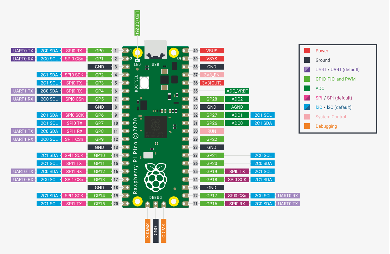
The Raspberry Pico is a development board with an RP2040 microcontroller chip. It has 264KB of SRAM and 2MB of flash memory. Development for the Pico is versatile as the platform capable of being programmed in MicroPython, CPython, C, and Rust 13. The Pico has a dual core processor capable of 133MHz clock speed, set to 125MHz out of the box 15. There are 40 GPIO pins on the board, with SPI, I2C, and UART communication capability. The Pico comes equip with a 12-bit 500ksps ADC with 5 channels total. One channel is configured to an RP2040 internal temperature sensor, and three are tied to GPIO pins on the Pico 14. The Pico also has a timer with four alarms, a Real-Time-Counter (RTC), and sixteen Pulse-Width Modulation (PWM) channels
ADC Theory
Analog to Digital Converters are the primary method of capturing analog data using a microcontroller. ADC’s capture analog signals such as sound or light waveforms and convert them to a digital signal for processing of information. An ADC takes continuous magnitude data from a continuous time domain into discrete magnitude data in a discrete time domain 3. The conversion quantizes the signal based on the resolution, reference voltages, and sample rate of the ADC, introducing small errors into the signal as noise.
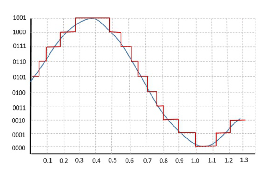
Quantization of an Analog to Digital Converter on a sine wave.
Resolution and reference voltages of an ADC produces quantization errors within the amplitude domain of a signal, where the sample rate of an ADC produces quantization errors within the time domain. Resolution gives the number of discrete values an ADC can produce, where the reference voltages provide the span of voltages the ADC can receive as a signal. Ground is often defaulted to the lower reference voltage to simplify ADC implementation. As a result, the voltage resolution in volts per bit is given as the span between the reference voltages divided by the number of discrete values the ADC resolution can produce. The digital code made by the ADC multiplied by the voltage resolution of the ADC will return the voltage recorded by the ADC. Quantization produces rounding errors in the approximation of the analog voltage, which is worsened by noise and jitter that exists on the signal prior to the ADC conversion. Signal noise can significantly reduce the effective number of bits to which an ADC is accurate.
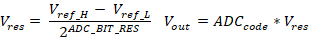
ADC formulas.
Sample rate of an ADC produces quantization errors within the time domain of the signal. The sampling rate of an ADC should ideally greater than twice the highest frequency being recorded, otherwise aliasing will occur. Aliasing can also be mitigated by adding a low-pass filter to the ADC input, removing frequencies above half of the sampling frequency. Oversampling is also commonly employed as it can reduce noise and improve bit-depth.
ADC Configuration
Since the ADC in on the Raspberry Pico, initial setup of the ADC can easily be achieved using the ADC section of the Pico Software Development Kit (SDK) 14. This provides the engineer with a simple and straightforward introduction on taking ADC readings. However, the 12-bit ADC onboard the Pico is not great by any means. This is due to the switching power regulator on the Pico. As a result of switching signal noise, the onboard voltage reference for the ADC is setup in poor conditions. The ADC has a 30mV offset and its signal is quite noisy 13. The datasheet gives suggestions on improvement of the ADC readings. An External reference voltage may be used, the R7 resistor can be removed, or issues can be mitigated in averaging and offset code. I chose a different route entirely, by adding bypass capacitors to the reference voltage and ADC input pins for filtering and smoothing. This is enough for the applications of this project.
SPI Theory
SPI is a full-duplex serial communication protocol that was created by Motorola in the 1980’s for high-speed communication in embedded systems 16. The SPI protocol consists of a single master device and one or many slave devices. For a simple two device system, A clock (SCLK), a chip select (CS), and two data lines (MOSI, MISO) are employed. MOSI is the data transmitted from the master device, while MISO is the data received from the master device.
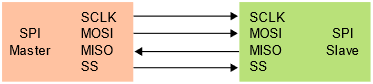
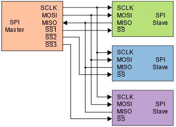
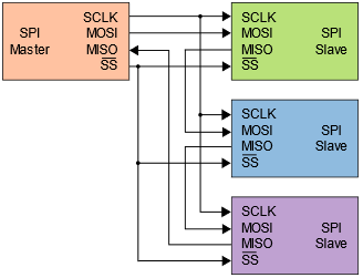
SPI can incorporate multiple slave devices by connecting data and clock lines, individually accessing a slave device by using a dedicated chip select line for each device as seen in figure 5. This can become GPIO intensive as the number of pins needed on the master device will increase with each additional slave device. Alternatively, SPI devices can work cooperatively by tying all chip selects to the same line as seen in figure 6. This works well if data does not need to be returned from the slave devices and the slave devices are intended to have the same output.
|
|
Figure 5: SPI independent configuration 16. |
Figure 6: SPI daisy-chained configuration 16. |
SPI transmits and receives data simultaneously in both directions, making the communication full duplex in design. SPI also uses GPIO for addressing a chip instead of transmitting addresses over the data lines commonly seen in I2C. Because of the full duplex data transmission and GPIO addressing, SPI has very high transmission speeds, but can become GPIO intensive. In practice, the maximum clock speeds of a SPI configuration depend highly on the connected devices and their method of connection. Finally, the SPI protocol is highly configurable in that the clock polarity and phase can be configured. This is also highly dependent on connected devices and should be considered when creating a two-device or multi-device system. In terms of using SPI on the Pico, A clock at or below 1MHz is best for breadboarding and flywire use.
DAC Theory
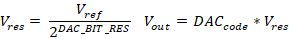
A Digital to Analog Converter operates on much of the same principles of an ADC but in reverse. DAC’s take a digital code that is within the resolution range of the device and output an analog waveform. Uses for DAC’s are often found in creating audio and video signals 4. A DAC will have a singular or pair of voltage references and a bit resolution for characterizing the precision and range of the output waveform. An output voltage can be calculated by dividing a given code by the number of discrete values the DAC can produce. This is then multiplied by the reference voltage to return the ideal output voltage.
DAC formulas.
DAC’s have some non-idealities in the form of differential and integral non-linearity, which characterize the difference between two adjacent code values and the difference in the transfer characteristic, respectively.
DAC Configuration
The LTC1661 from Linear Technology hosts two 10-bit DAC’s that are addressable via SPI 3. Communication is configured with the SPI clock idling low and capturing data on the rising edge of the clock. Simple initialization of SPI on the Pico can be seen chapter 3.7 the MicroPython SDK 14. For an in-depth approach to SPI initialization and communication on the Pico, the MicroPython documentation for the SPI module proved insightful 12. The maximum baud rate of the LTC1661 is 10MHz 10. I employed a baud rate of no larger than 8MHz to avoid data corruption on the breadboard. However, small distances of SPI connections on the final PCB make higher speeds possible. The default SPI pins of the Pico were employed, located the bottom right corner of the Pico Pinout 13.
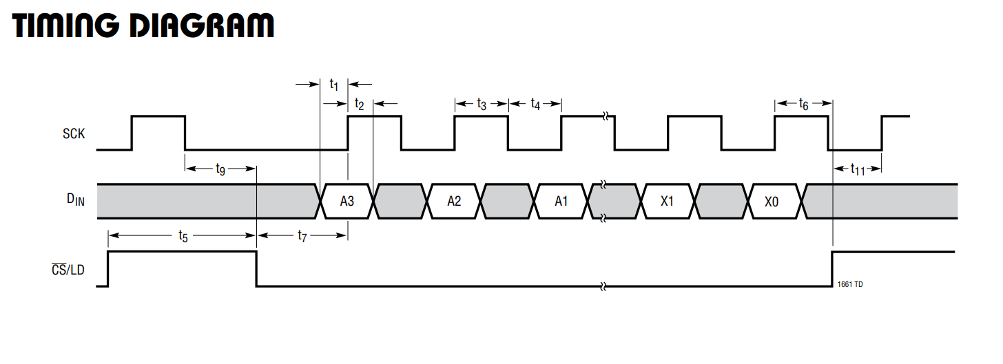
Communication with this DAC is slightly more complicated due to the 10-bit resolution associated with the device. Commanding the device to write to its internal register and Update is the primary functionality desired for this module. Knowing this, the commands 0x9 or 0xA would be applicable for continuously changing voltage on output A and B respectively 10
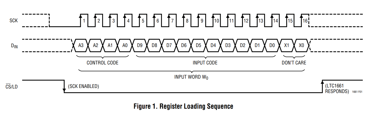
In our program, we must parse the data for every transmission so that a word packet sent will have the format seen in figure 9. The LTC1661 sends the command, then splits the data bits between the two bytes, followed by don’t cares to fill the word packet. In an 8-, 12-, or 16-bit DAC, less bit manipulation is required.
Operational Amplifier Theory
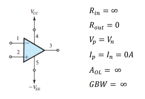
Operational Amplifiers (Op-Amps) are high-gain voltage amplifiers with differential input and a single voltage output. Op-Amps typically have five terminals: An inverting input, non-inverting input, an upper supply, a lower supply, and an output. An ideal Op-Amp has an infinite input resistance and zero output resistance. As a result, input terminals see zero current. Input terminals also see equivalent voltages. Lastly, ideal op-amps experience infinite open-loop gain and infinite Gain Bandwidth (GBW).
Using an infinite open-loop gain is limiting, as the output voltage signal would become saturated immediately. This could be useful in a comparator circuit. However, for most purposes some form of negative feedback is implemented to create a closed loop gain within the boundaries of the supply rails. Negative feedback amplifiers come in inverting (Figure 11) and non-inverting (Figure 12) configurations, with gain determined by the ratio of resistances seen by the negative feedback loop.
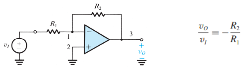
Inverting Op-Amp configuration and voltage gain equation 1.
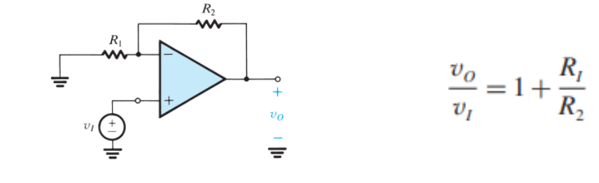
Non-inverting Op-Amp configuration and voltage gain equation 1.
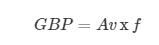
Non-idealities of real-life Op-Amps will also affect the circuit, the most influential of which is determined by a given IC’s strengths and weaknesses. A notable non-ideality can be seen in gain bandwidth and subsequent frequency response. Finite GBW/GBP of an Op-Amp produces attributes of an active lowpass filter. With the lower cutoff frequency determined by the GBP divided by the gain of the circuit 5. As a result, open-loop response often has high gain with very low cutoff frequency. Whereas closed-loop gain will keep gain approximately constant for a much wider bandwidth.
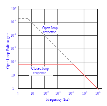
LM741 Frequency response in open and closed loop configurations 7.
Other non-idealities of Op-Amps are limits on output current, voltage, and slew rate. Output voltage can become saturated due to voltage gain exceeding the supply rails. Current supplied by an Op-Amp IC is highly dependent on a model, and current limits may be imposed for safety of the internal circuitry. The maximum rate of change for an Op-Amps output voltage is referred to as its slew rate. Op-Amps are slew rate limited at frequencies of operation that require a faster rate than the IC can permit.
First-Order Filter Theory
Analog filters are a method of reducing gain of responses at certain frequencies. First-order filters implement a singular cutoff frequency while second order filters implement multiple cutoff frequencies. Filters can be implemented in active and passive configurations, meaning with and without Op-Amps respectively. Regardless of a filter being passive or active, Filter frequencies and modes of operation are created between RL and RC components. Figure 15 implements passive and active filters in multiple filter configurations.
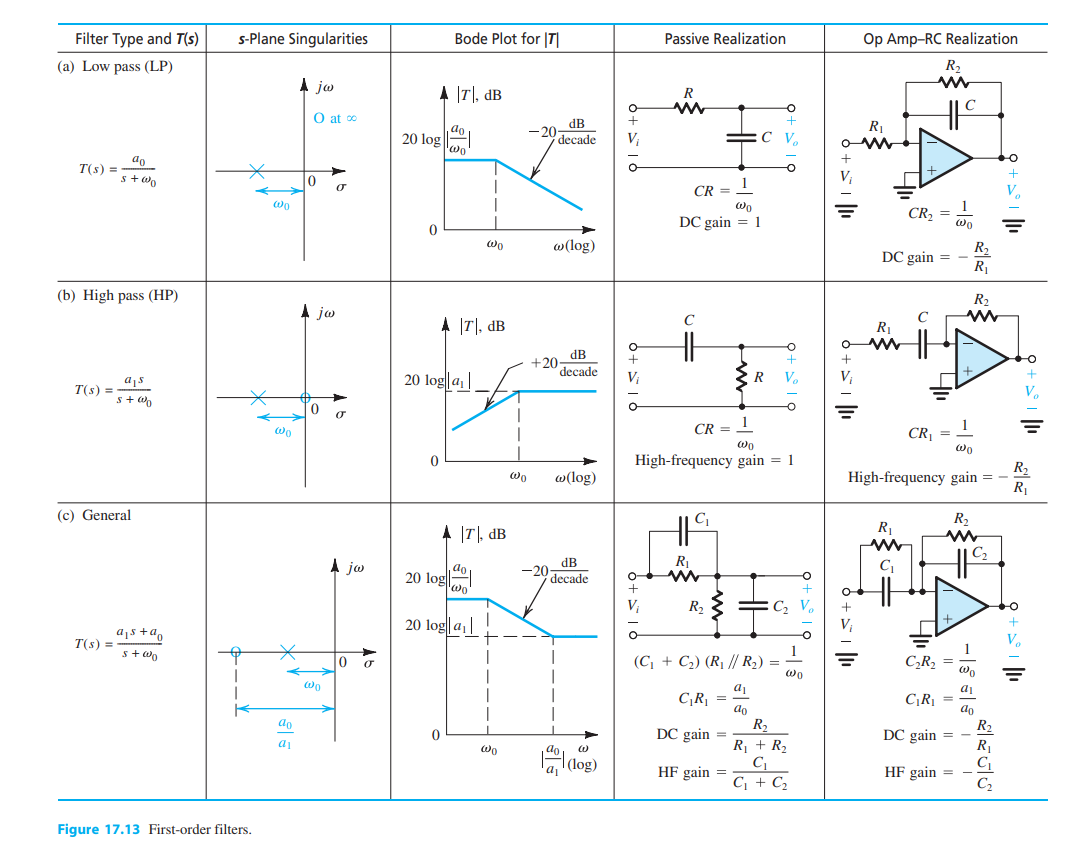
First order filter table with active and passive applications 1.
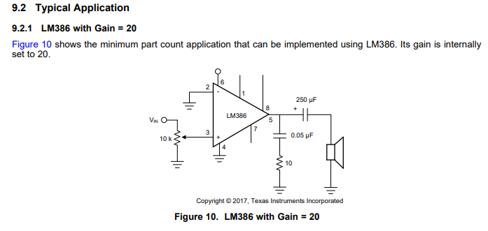
Audio Amplifier Configuration
The audio amplifier circuit has a simple implementation. The primary goal was creating a circuit with 26dB gain (20V/V) using the LM386. This was easily accomplished by referring to the LM386 datasheet as they provide applications in section 9 of the document (Figure 16) 9. Implementation can be seen on the schematic, Figure 22. I made no changes to the circuit recommended by the datasheet.
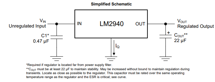
Power Regulation and Filtering
To supply power to the system, I chose to use the LM2940 5V low-dropout regulator. This allows for a 9-12V DC source to supply the devices without much overhead. This provided a smooth 5V source for most components, with local decoupling capacitors where needed. The LM2940 is a prime candidate for 5V regulation as its implementation is simple, only requiring two capacitors on the Vin and Vout 8. I implemented an array of values for the output capacitors out of an abundance of safety and a desire for a highly filtered power source 2, 18.
In addition to the 5V source, I powered the Raspberry Pico via the VSYS node to activate the device and use the 3.3V Switching Mode Power Supply (SMPS). This was done using a Schottky diode from 5V to VSYS to avoid backflow when the Pico is plugged in via USB 13. The Pico power-chain is good because the SMPS is efficient, but noise on the output causes problems with other systems like the ADC 13, 14. As a result, I added bypass capacitors to this source as well.
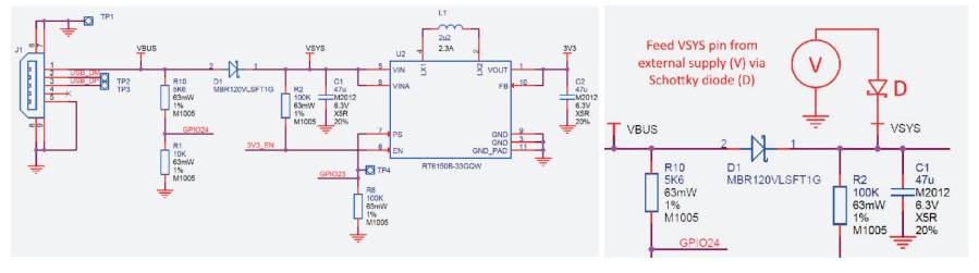
Pico Power-chain and the implemented method of external supply 8.
Inputs and Outputs
Buttons, switches, and LEDs are integrated into the design for various controls and system status. All inputs are setup in a pull-down configuration. Wave selection is controlled by the active switches while both menu selection and software resets are controlled by the buttons. This allows for a robust interface system to be implemented in software. GPIO selected for these pins were selected last to ensure critical systems had placement. Button debouncing was taken care of in software by implementing a delay after initial triggering. Alternatively, these buttons could be debounced using small bypass capacitors such as a 100nF, creating a linear voltage response for the IO pin instead of a bouncing signal. All buttons, switches, and output LED’s use the 3.3V source from the SMPS as to not damage GPIO pins on the Pico. They are also paired with 220-ohm resistors to give the LED’s maximum brightness in a safe current range.
Ultrasonic Sensors
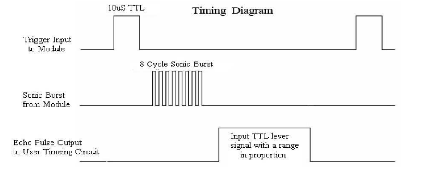
The HC-SR04 is an Ultrasonic sensor module that uses sonar to determine distance of objects similar to echolocation seen in animals like bats or dolphins 6. It is rated for distances of 2cm to 400cm and can provide high accuracy within this range. The sensors have four connections, VCC, Trig, Echo, and GND. The device operates with a 5V supply, while the trigger and echo are used to communicate digital data between the sensor and a microcontroller.
From the microcontroller, the Trig pin is set high for 10uS then brought low. This tells the sensor to send eight 40kHz bursts from the transmitter. The microcontroller should then poll the Echo pin, waiting for a high signal from the receiver, indicating the return of the bursts echo. The time between the rising and falling edge of the Echo pin can be used to calculate distance based on the speed of sound, 343 m/s. Based on the distances calculated from each sensor, we can modify output sound data.
LCD Configuration
Configuration of the Crystal Fontz AH1602Z-YYH for parallel communication was a major step in setup of this circuit. I chose to use parallel communication to interact with the LCD as opposed to SPI or I2C for simplicity and use of previous code. The LCD is wired in parallel to the microcontroller with four-bit communication 17. A potentiometer was connected for contrast control of the LCD, and a photoresistor and 1k-ohm resistor was connected in parallel for adaptive brightness control. For parallel communication, a nibble of data is sent to the display simultaneously. Full bytes of data are then sent to the device in a process called bit-banging. This splits a byte of data to send two nibbles in series, communicating the upper four bits and then the lower four bits. For wiring of the device, previous lecture slides and LCD driver manual were helpful in wiring and debugging issues with contrast and brightness 17.
Theremin Circuit Configuration
The various components are connected in a circuit following the hardware diagram and schematics seen below. 9V Power is connected via a barrel jack and regulated to 5V, supplying the Pico through a Schottky diode. An LED is also driven by the 5V rail to indicate a power on status and a switch is present to cut off the 9V power to the circuit entirely. The 3.3V output of the Pico is used for all buttons, switches, and output LEDs. Two potentiometers are connected between 3.3V and ground with the wiper connecting to ADC pins, allowing variable analog input to the system. Switches, Buttons, and output LEDs are 3.3V pull-downs available for menu and waveform controls.
The DAC and audio amplifier are connected in series, followed by an 8-ohm speaker, presenting the Analog output waveform. Another potentiometer was connected between the DAC and amplifier to provide a coarse volume control on the output. Digital output in the form of Status LEDs indicate continuous operation by toggling and display on reset of the device.
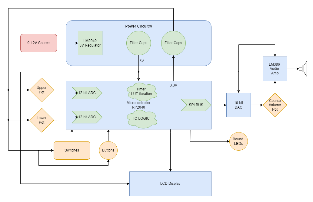
Hardware Block Diagram of the Theremin Circuit.
A single processor flow was employed for reliability and simplicity. To help speed up operations, a generous overclock was applied, setting the system clock to 270MHz. The Pico would start by initializing SPI communication at 10MHz, LCD parallel communication, and Ultrasonic sensor communication. This was followed by all other GPIO initialization, definition of button interrupts, and creating the waveform generation process in the timer tick.
The Pico would then enter its program loop, where a startup splash screen would be displayed along with lighting all LEDs. All variables would also be set to their default state. Pressing the reset button would return the user to this point in the program.
The main loop would then be entered and would continue until the reset button is pressed. In this process, the ADC, ultrasonic sensors, and switches are all polled for data. Depending on the state of the display menu set by button interrupts, the ADCs could set the frequency or amplitude range for computation later. The LCD prints a display associated with the current menu state. If both sensors detect the hands of the user, frequency and amplitude is then calculated based on the current boundaries for each and the ultrasonic sensor data. The timer is then started or adjusted for frequency shifts, and the processor sends SPI data to the DAC for output. If the sensors do not detect objects or a waveform is not selected with a switch, sound will not be output. Lastly, the onboard LED is toggled and the loop restarts for the duration of instrument use.
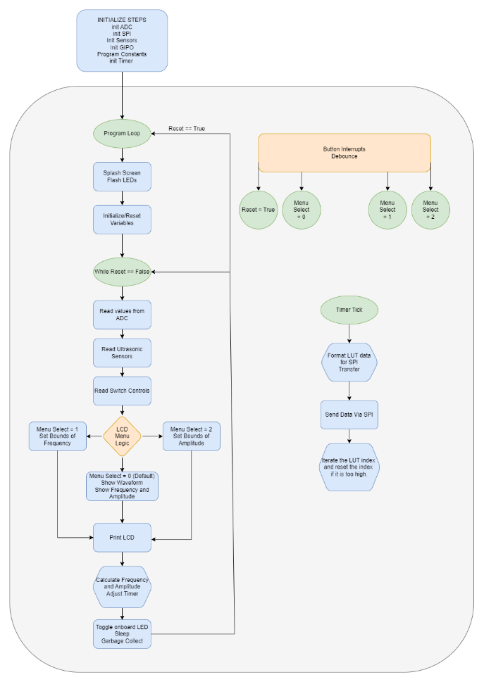
Software Block Diagram of the Theremin Circuit.
Schematic and PCB Design
All previously mentioned components must be compiled into a schematic design for wiring structure and PCB design. Useful tips and tricks for understanding the Altium can be learned by watching Professor Stapleton’s videos 11.
The most useful design points are regarding power and capacitor placement. Bypass and decoupling capacitors are added to the board for several reasons. First, capacitors can be used on power headers to avoid voltage spikes and removing AC ripple on DC power. Small ceramic caps offer low series resistance and react fast but have a difficult time dealing with substantial amounts of charge over long periods. Polarized electrolytic capacitors usually have a much higher capacitance, and in conjunction with smaller ceramic capacitors, effectively clean DC voltage 2, 11. In larger schematics and PCB’s, we are not always able to position circuits near bypass capacitors. Therefore, small decoupling capacitors are recommended for placement near a circuit subsection to help clean AC ripple from DC voltages 2.
Once the schematic was populated with all necessary circuit components, the PCB was updated with all schematic components for board layout. A general layout of parts was done before resizing the board outline to find the most effective use of space. When all components have found their relative placement, routing traces for components using auto-routing tools or manually is required. I chose to auto-route, followed with manual edits to correct some trace routes. I found 20mil routes were sufficient for this circuit. Copper pours are also recommended for adding a ground or Vcc layer to the PCB, further simplifying routing design and common routes. I implemented a Ground and 5V layer using the copper pours.
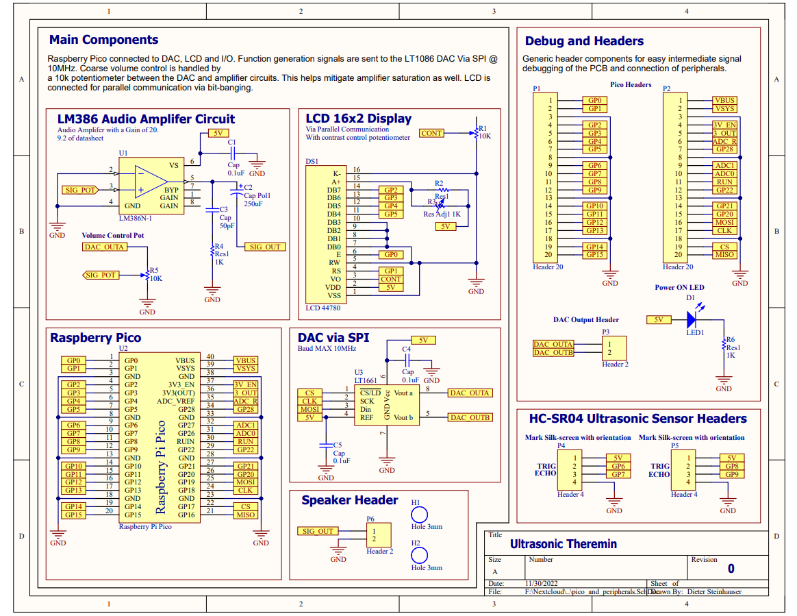
Ultrasonic Theremin schematic page 1 of 2.
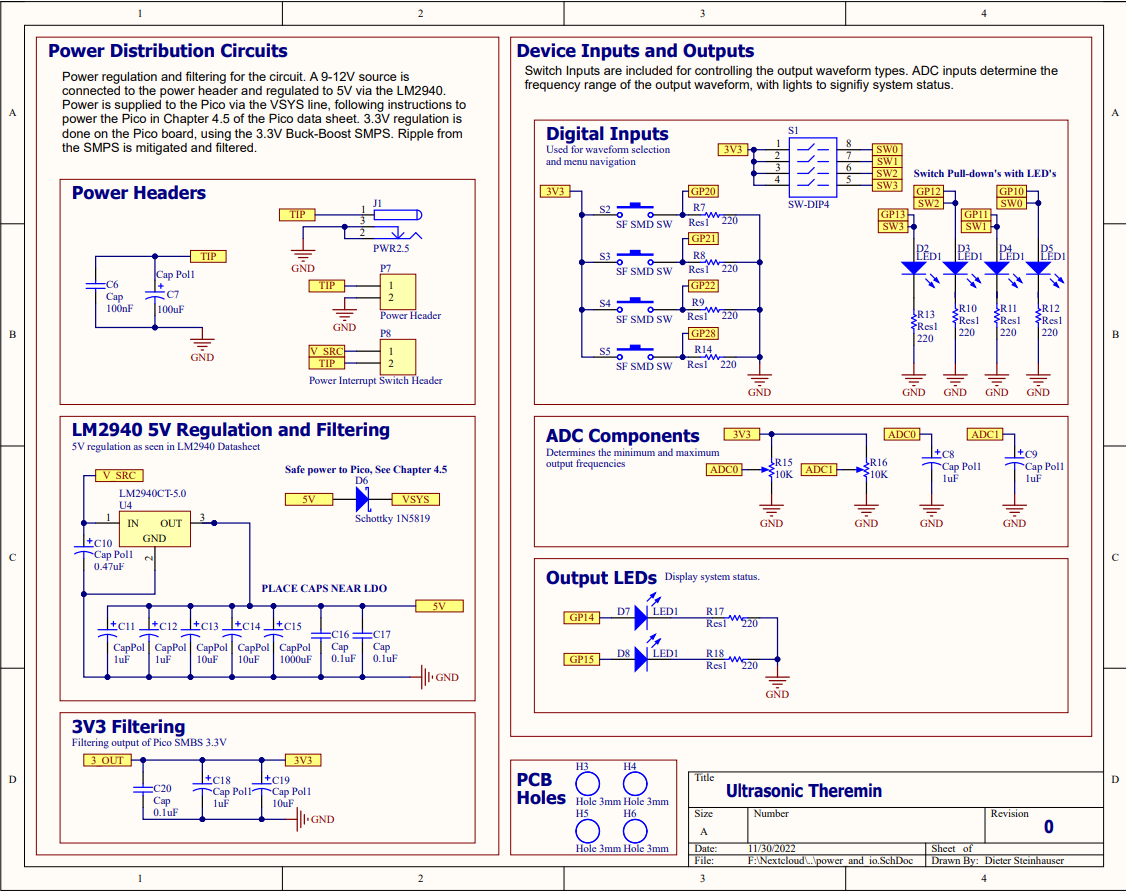
Ultrasonic Theremin schematic page 2 of 2.
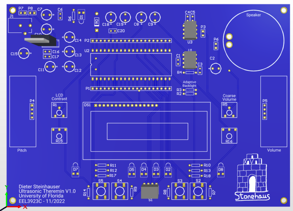
Top side of Ultrasonic Theremin PCB layout.
Bill Of Materials
Name |
Description |
Designators |
Quantity |
Price |
Component Total |
1000uF Cap |
Electrolytic Capacitor |
C15 |
1 |
$1.60 |
$1.60 |
270uF Cap |
Electrolytic Capacitor |
C2 |
1 |
$0.33 |
$0.33 |
100uF Cap |
Electrolytic Capacitor |
C7 |
1 |
$0.09 |
$0.09 |
10uF Cap |
Electrolytic Capacitor |
C13, C14, C19 |
3 |
$0.07 |
$0.21 |
1uF Cap |
Electrolytic Capacitor |
C8, C9, C11, C12, C18 |
5 |
$0.06 |
$0.30 |
0.47uF Cap |
Electrolytic Capacitor |
C10 |
1 |
$0.09 |
$0.09 |
0.1uF Cap |
Ceramic Capacitor |
C1, C4, C5, C6, C16, C17, C20 |
7 |
$0.09 |
$0.63 |
50pF Cap |
Ceramic Capacitor |
C2 |
1 |
$0.17 |
$0.17 |
10K Pots |
3-pin Potentiometer |
R1, R5, R15, R16 |
4 |
$1.13 |
$4.52 |
1K Res |
axial Resistor |
R2, R4, R6 |
3 |
$0.05 |
$0.15 |
220 Res |
axial Resistor |
R7, R8, R9, R10, R11, R12, R13, R14, R17, R18 |
10 |
$0.03 |
$0.28 |
Photoresistor |
Photoresistor |
R3 |
1 |
$1.18 |
$1.18 |
LEDs |
5mm LED |
D1, D2, D3, D4, D5, D7, D8 |
7 |
$0.09 |
$0.63 |
LCD44780 |
16x2 LCD Display |
DS1 |
1 |
$6.27 |
$6.27 |
LTC1661 |
10bit DAC |
U3 |
1 |
$6.21 |
$6.21 |
LM386 |
Audio Amplifier |
U1 |
1 |
$1.50 |
$1.50 |
8 Ohm Speaker |
8 Ohm Speaker |
P6 |
1 |
$4.68 |
$4.68 |
LM2940 |
5V LDO Regulator |
U4 |
1 |
$2.70 |
$2.70 |
1N5819 |
Schottky Diode |
D6 |
1 |
$0.28 |
$0.28 |
9V Adapter |
AC/DC Adapter |
N/A |
1 |
$7.99 |
$7.99 |
Barrel Jack |
Female Connector |
P7 |
1 |
$0.71 |
$0.71 |
SPST Switch |
SPST Switch |
P8 |
1 |
$2.15 |
$2.15 |
HC-SR04 |
Ultrasonic Sensors |
P4, P5 |
2 |
$3.75 |
$7.50 |
Pico |
Raspberry Pico uP |
U2 |
1 |
$4.00 |
$4.00 |
SW_DIP 4 |
DIP Switch package |
S1 |
1 |
$0.59 |
$0.59 |
Buttons |
Buttons |
S2, S3, S4, S5 |
4 |
$1.18 |
$4.72 |
Project Total: |
$59.48 |
Results
The schematic of the circuit and PCB turned out well, with minimal errors. The assembled PCB was easy to debug because of its plentiful headers employed in the diagram. Also, using female headers for the ultrasonic sensors, LCD, DIP packages, and potentiometers aided debug and ensured that any errors in design could be more easily fixed if the PCB was routed wrong. Thankfully, there were no design breaking errors in this circuit, and most components worked immediately after installation.
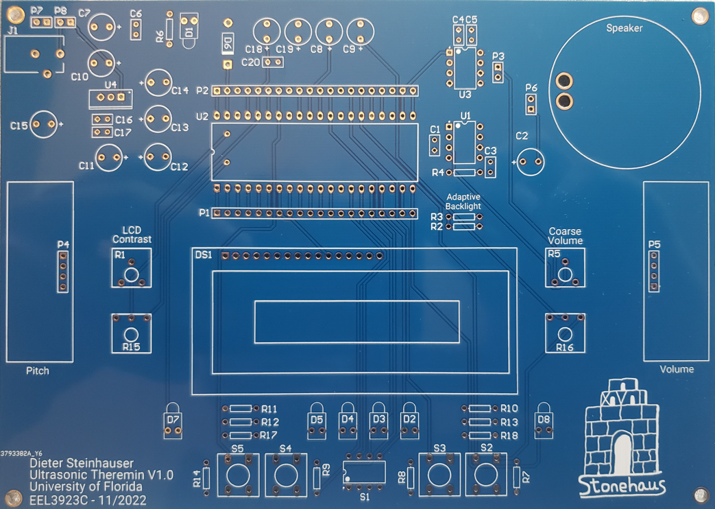
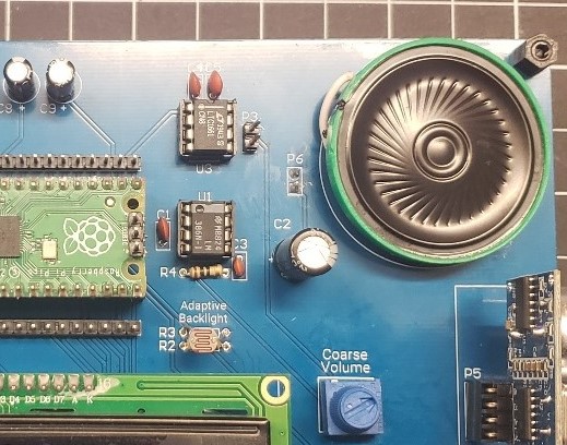
Empty Theremin Circuit PCB.
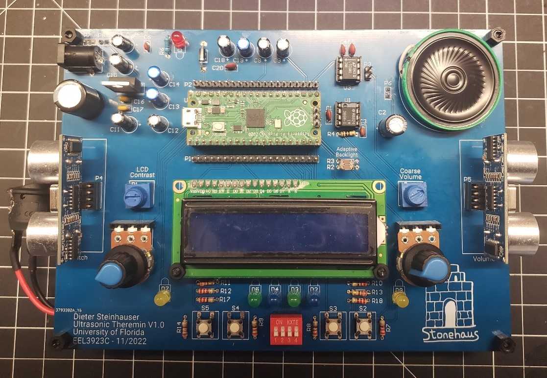
Populated Theremin Circuit PCB.
Power
The power regulation and filtering produced a 5V source with minimal noise, observed with as little as 10mV ripple on the source. Extra filtering on the 3.3V source also seemed fruitful but may benefit from a larger array of capacitances to further smooth the ~30-40mV ripple observed on the device pin. This is a slight improvement on the unfiltered 3.3V rail.
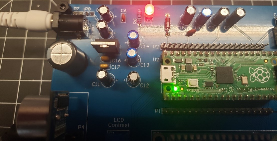
Power regulation system on the PCB

5V source observed on the oscilloscope.

3.3V source observed on the oscilloscope.
Audio
The audio system of this circuit had no issue driving the 8-ohm speaker for a variety of 32-step waveforms. The coarse volume potentiometer helped easily remove clipping from the amplifier stage. Frequencies of 160Hz were achievable with system stability. Frequencies up to 240 were achieved using this audio configuration, however this boost is audio transaction demand.
Without Speaker Load
Audio output system.

Sine wave output of the Audio Amplifier without speaker load.

Square wave output of the Audio Amplifier without speaker load.

Triangle wave output of the Audio Amplifier without speaker load.

Sawtooth wave output of the Audio Amplifier without speaker load.
With Speaker Load
The audio amplifier with an 8-ohm speaker creates an RC circuit, and adds capacitive loading and unloading. Slight hiccupping of the output waveform can also be observed due to issues with the python interpreter, as well as variation in frequency/amplitude from ultrasonic sensors when sampling.

Sine wave output of the Audio Amplifier with speaker load.

Square wave output of the Audio Amplifier with speaker load.

Triangle wave output of the Audio Amplifier with speaker load.

Sawtooth wave output of the Audio Amplifier with speaker load.
Interface and Display
The finished theremin circuit displayed its menu system intuitively. On startup, the splash screen displays the project name and system clock, while holding the yellow and onboard LEDs high. After the splash screen, the system hits the home screen to display waveform, frequency, and amplitude readings in real time. DIP switches control the wave types, allowing sine, square, triangle, and sawtooth from left to right. Once both sensors detect objects, they display the potential frequency and amplitude of the wave. The output signal is only generated when both sensors detect, and a waveform switch is selected.
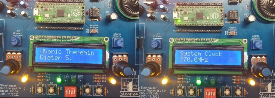
Splash screen on system reset.
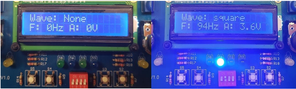
Home screen with waveform selection, frequency, and amplitude readings.
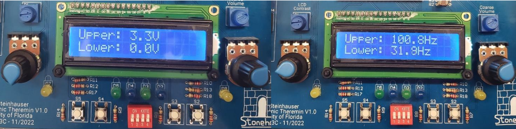
Amplitude and frequency boundary menu.
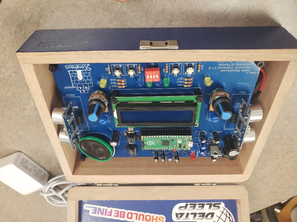
Ultrasonic Theremin in its case.
Close up of the ultrasonic theremin in its case.
Discussion
Overall, the ultrasonic theremin circuit was a success. It has some minor problems that can be solved with small modifications to the PCB or software, but performs its task as expected. In terms of the power system, the regulation of the 5V source was excellent, however my smoothing of the 3.3V leaved something to be desired. This could be improved upon by adding more capacitance on the output rail. However, for our purposes of the 3.3V rail this is unnecessary. If I was to use the onboard ADC for more detail-oriented measurements, I would consider using an external LDO for 3.3V regulation, or work on filtering this 3.3V rail more. Regarding layout and the schematic, I believe that the design worked very well. There are minor changes for ease of use I would make with more time. These issues include moving C12 out of the Pico’s USB port area, taking more time to implement exact potentiometer footprints, and creating larger holes for the speaker wires.
The audio output system could be improved by adding a coupling capacitor on the signal line between the DAC and the LM386, as well as removal of the potentiometer from the signal path to reduce noise. With the removal of the potentiometer, it could alternatively be placed on the DAC reference to provide a similar result and reduce signal noise. LM386 amplification and filtering could be improved slightly, but for the purposes of this device I believe the current configuration is sufficient and could be improved mostly by my former critiques. Frequency range could also be improved by exploring multithreading, DMA, or other software efficiency systems to isolate data transactions to the DAC. Not exploring these avenues leaves considerable improvement available on the software architecture, but overclocking allowed for a proof of concept in demonstration.
Ultimately, the ultrasonic theremin was an interesting and unique project. We applied a variety of systems to bring together a working solution. Hardware included concepts of power regulation and filtering, I/O, LCD data display, and analog amplification. Software concepts of ADC and DAC conversions, interrupt service routines, debouncing, hardware timers, overclocking, parallel and SPI communication, and lookup tables were Implemented. Most systems were implemented well enough to meet project requirements and expectations. Room for improvement leaves potential for a revision of both the circuit and code, allowing for easier use, higher frequencies, and better responsiveness.
Appendix
LCD.py
  1# -----------------------------------------
  2#                 NOTES
  3# -----------------------------------------
  4"""
  5Dieter Steinhauser
  65/2023
  7Parallel LCD functions, Configured for 4-bit communication.
  8"""
  9
 10# -----------------------------------------
 11#               IMPORTS
 12# -----------------------------------------
 13
 14from machine import Pin
 15import utime
 16
 17# -----------------------------------------
 18#          CONSTANTS AND VARIABLES
 19# -----------------------------------------
 20
 21# CONSTANTS
 22# ----------------------
 23
 24LCD_CMD = 0
 25LCD_DATA = 1
 26
 27# ----------------------
 28# GPIO Wiring: Legacy Structure
 29# ----------------------
 30
 31EN = Pin(0, Pin.OUT) # Enable Pin
 32RS = Pin(1, Pin.OUT) # Register Select
 33
 34PINS = [5, 4, 3, 2]
 35# Pin numbers for the upper nibble, does the below assignment in configure method.
 36# D4 = Pin(2, Pin.OUT)
 37# D5 = Pin(3, Pin.OUT)
 38# D6 = Pin(4, Pin.OUT)
 39# D7 = Pin(5, Pin.OUT)
 40
 41# list that gets populated with pinout objects for data line.
 42DATA_BUS = []
 43
 44# -----------------------------------------
 45#                 METHODS
 46# -----------------------------------------
 47
 48def Configure():
 49    """Creates the data bus object from the pin list"""
 50
 51    for index in range(4):
 52       DATA_BUS.append(Pin(PINS[index], Pin.OUT))
 53
 54# -----------------------------------------
 55
 56def lcd_strobe():
 57    """Flashes the enable line and provides wait period."""
 58
 59    EN.value(1)
 60    utime.sleep_ms(1)
 61
 62    EN.value(0)
 63    utime.sleep_ms(1)
 64
 65# -----------------------------------------
 66
 67def lcd_write(command, mode):
 68    """Sends data to the LCD module. """
 69
 70    # determine if writing a command or data
 71    data = command if mode == 0 else ord(command)
 72
 73    # need upper nibble for first loop. lower nibble can use data directly.
 74    upper = data >> 4
 75
 76    # write the upper nibble
 77    for index in range(4):
 78        bit = upper & 1
 79        DATA_BUS[index].value(bit)
 80        upper = upper >> 1
 81
 82    # strobe the LCD, sending the nibble
 83    RS.value(mode)
 84    lcd_strobe()
 85
 86    # write the lower nibble
 87    for index in range(4):
 88        bit = data & 1
 89        DATA_BUS[index].value(bit)
 90        data = data >> 1
 91
 92    # Strobe the LCD, sending the nibble
 93    RS.value(mode)
 94    lcd_strobe()
 95    utime.sleep_ms(1)
 96    RS.value(1)
 97
 98# -----------------------------------------
 99
100def lcd_clear():
101    """Clear the LCD Screen."""
102
103    lcd_write(0x01, 0)
104    utime.sleep_ms(5)
105
106# -----------------------------------------
107
108def lcd_home():
109    """Return the Cursor to the starting position."""
110
111    lcd_write(0x02, 0)
112    utime.sleep_ms(5)
113
114# -----------------------------------------
115
116
117def lcd_cursor_blink():
118    """Have the cursor start blinking."""
119
120    lcd_write(0x0D, 0)
121    utime.sleep_ms(1)
122
123# -----------------------------------------
124
125def lcd_cursor_on():
126    """Have the cursor on, Good for debugging."""
127
128    lcd_write(0x0E, 0)
129    utime.sleep_ms(1)
130
131# -----------------------------------------
132
133def lcd_cursor_off():
134    """Turn the cursor off."""
135
136    lcd_write(0x0C, 0)
137    utime.sleep_ms(1)
138
139# -----------------------------------------
140
141def lcd_puts(string):
142    """Write a string on to the LCD."""
143
144    for element in string:
145       lcd_putch(element)
146
147# -----------------------------------------
148
149def lcd_putch(c):
150    """Write a character on to the LCD."""
151    lcd_write(c, 1)
152
153# -----------------------------------------
154
155def lcd_goto(column, row):
156
157
158    if row == 0:
159        address = 0
160
161    if row == 1:
162        address = 0x40
163
164    if row == 2:
165        address = 0x14
166
167    if row == 3:
168        address = 0x54
169
170    address = address + column
171    lcd_write(0x80 | address, 0)
172
173# -----------------------------------------
174
175def lcd_init():
176
177    # Configure the pins of the device.
178    Configure()
179    utime.sleep_ms(120)
180
181    # clear values on data bus.
182    for index in range(4):
183        DATA_BUS[index].value(0)
184    utime.sleep_ms(50)
185
186    # initialization sequence.
187    DATA_BUS[0].value(1)
188    DATA_BUS[1].value(1)
189    lcd_strobe()
190    utime.sleep_ms(10)
191
192    lcd_strobe()
193    utime.sleep_ms(10)
194
195    lcd_strobe()
196    utime.sleep_ms(10)
197
198    DATA_BUS[0].value(0)
199    lcd_strobe()
200    utime.sleep_ms(5)
201
202    lcd_write(0x28, 0)
203    utime.sleep_ms(1)
204
205    lcd_write(0x08, 0)
206    utime.sleep_ms(1)
207
208    lcd_write(0x01, 0)
209    utime.sleep_ms(10)
210
211    lcd_write(0x06, 0)
212    utime.sleep_ms(5)
213
214    lcd_write(0x0C, 0)
215    utime.sleep_ms(10)
216
217
218# -----------------------------------------
219#                 LCD Class:
220# -----------------------------------------
221
222
223class LCD:
224    """The LCD class is meant to abstract the LCD driver further and streamline development."""
225
226    CMD_MODE = 0
227    DATA_MODE = 1
228
229    def __init__(self, enable_pin: int, reg_select_pin: int, data_pins: list) -> None:
230        """Object initialization"""
231
232        self.enable_pin = Pin(enable_pin, Pin.OUT)
233        self.reg_select_pin = Pin(reg_select_pin, Pin.OUT)
234        self._data_pins = data_pins
235        self.data_bus = []
236
237        # Configure the pins of the device.
238        self._configure()
239        utime.sleep_ms(120)
240
241    # -----------------------------------------
242
243    def _configure(self):
244        """Creates the data bus object from the pin list. """
245
246        # Configure the pins of the device.
247        for element in self._data_pins:
248            self.data_bus.append(Pin(element, Pin.OUT))
249
250    # -----------------------------------------
251
252    def init(self):
253        """Initializes the LCD for communication."""
254
255        # clear values on data bus.
256        for index in range(4):
257            self.data_bus[index].value(0)
258        utime.sleep_ms(50)
259
260        # initialization sequence.
261        self.data_bus[0].value(1)
262        self.data_bus[1].value(1)
263        self.strobe()
264        utime.sleep_ms(10)
265
266        self.strobe()
267        utime.sleep_ms(10)
268
269        self.strobe()
270        utime.sleep_ms(10)
271
272        self.data_bus[0].value(0)
273        self.strobe()
274        utime.sleep_ms(5)
275
276        self.write(0x28, 0)
277        utime.sleep_ms(1)
278
279        self.write(0x08, 0)
280        utime.sleep_ms(1)
281
282        self.write(0x01, 0)
283        utime.sleep_ms(10)
284
285        self.write(0x06, 0)
286        utime.sleep_ms(5)
287
288        self.write(0x0C, 0)
289        utime.sleep_ms(10)
290
291    # -----------------------------------------
292
293    def strobe(self):
294        """Flashes the enable line and provides wait period."""
295
296        self.enable_pin.value(1)
297        utime.sleep_ms(1)
298
299        self.enable_pin.value(0)
300        utime.sleep_ms(1)
301
302    # -----------------------------------------
303
304    def write(self, command, mode):
305        """Sends data to the LCD module. """
306
307        # determine if writing a command or data
308        data = command if mode == 0 else ord(command)
309
310        # need upper nibble for first loop. lower nibble can use data directly.
311        upper = data >> 4
312
313        # write the upper nibble
314        for index in range(4):
315            bit = upper & 1
316            self.data_bus[index].value(bit)
317            upper = upper >> 1
318
319        # strobe the LCD, sending the nibble
320        self.reg_select_pin.value(mode)
321        self.strobe()
322
323        # write the lower nibble
324        for index in range(4):
325            bit = data & 1
326            self.data_bus[index].value(bit)
327            data = data >> 1
328
329        # Strobe the LCD, sending the nibble
330        self.reg_select_pin.value(mode)
331        self.strobe()
332        utime.sleep_ms(1)
333        self.reg_select_pin.value(1)
334
335    # -----------------------------------------
336
337    def clear(self):
338        """Clear the LCD Screen."""
339
340        self.write(0x01, 0)
341        utime.sleep_ms(5)
342
343    # -----------------------------------------
344
345    def home(self):
346        """Return the Cursor to the starting position."""
347
348        self.write(0x02, 0)
349        utime.sleep_ms(5)
350
351    # -----------------------------------------
352
353
354    def blink(self):
355        """Have the cursor start blinking."""
356
357        self.write(0x0D, 0)
358        utime.sleep_ms(1)
359
360    # -----------------------------------------
361
362    def cursor_on(self):
363        """Have the cursor on, Good for debugging."""
364
365        self.write(0x0E, 0)
366        utime.sleep_ms(1)
367
368    # -----------------------------------------
369
370    def cursor_off(self):
371        """Turn the cursor off."""
372
373        self.write(0x0C, 0)
374        utime.sleep_ms(1)
375
376    # -----------------------------------------
377
378    def print(self, string):
379        """Write a string on to the LCD."""
380
381        for element in string:
382            self._putch(element)
383
384    # -----------------------------------------
385
386    def _putch(self, c):
387        """Write a character on to the LCD."""
388        self.write(c, 1)
389
390    # -----------------------------------------
391
392    def _puts(self, string):
393        """Write a string on to the LCD."""
394
395        for element in string:
396            self._putch(element)
397
398
399    # -----------------------------------------
400    def go_to(self, column, row):
401
402
403        if row == 0:
404            address = 0
405
406        if row == 1:
407            address = 0x40
408
409        if row == 2:
410            address = 0x14
411
412        if row == 3:
413            address = 0x54
414
415        address = address + column
416        self.write(0x80 | address, 0)
417
418
419# -----------------------------------------
420#              END OF FILE
421# -----------------------------------------
LUT.py
  1# -----------------------------------------
  2#                 NOTES
  3# -----------------------------------------
  4"""
  5
  6Dieter Steinhauser
  710/1/2022
  8Design 1
  9DAC Lookup Tables
 10
 11The following are lists of 32 and 256 words that assemble one period
 12of a waveform
 13"""
 14
 15# -----------------------------------------
 16#                 CONSTANTS
 17# -----------------------------------------
 18
 19FREQ_MAX = 100
 20FREQ_MIN = 10
 21DAC_WRITE_THRU_A = 0x9 << 12 # WRITE_THRU_A
 22DAC_WRITE_THRU_B = 0xA << 12 # WRITE_THRU_B
 23
 24# -----------------------------------------
 25#                 LUTS
 26# -----------------------------------------
 27
 28# 10 bit res
 29SQUARE_WAVE_LUT = [0]*16 + [1023]*16
 30
 31SQUARE_WAVE_LUT_256 = [0]*128 + [1023]*128
 32
 33
 34# 10 bit res
 35SAWTOOTH_WAVE_LUT = list(range(0, 1023, 32))
 36
 37SAWTOOTH_WAVE_LUT_256 = list(range(0, 1023, 4))
 38
 39
 40# 10 bit res
 41SINE_WAVE_LUT = [0x200,0x264,0x2c4,0x31c,0x36a,0x3aa,0x3d9,0x3f6,0x400,0x3f6,0x3d9,0x3aa,0x36a,0x31c,0x2c4,0x264,
 420x200,0x19c,0x13c,0xe4,0x96,0x56,0x27,0xa,0x0,0xa,0x27,0x56,0x96,0xe4,0x13c,0x19c]
 43
 44
 45SINE_WAVE_LUT_256 = [0x200,0x20c,0x219,0x225,0x232,0x23e,0x24b,0x257,0x263,0x270,0x27c,0x288,0x294,0x2a0,0x2ac,0x2b8,
 460x2c3,0x2cf,0x2da,0x2e5,0x2f1,0x2fc,0x306,0x311,0x31c,0x326,0x330,0x33a,0x344,0x34e,0x357,0x360,
 470x369,0x372,0x37a,0x383,0x38b,0x393,0x39a,0x3a2,0x3a9,0x3b0,0x3b6,0x3bd,0x3c3,0x3c8,0x3ce,0x3d3,
 480x3d8,0x3dd,0x3e1,0x3e5,0x3e9,0x3ec,0x3f0,0x3f3,0x3f5,0x3f7,0x3f9,0x3fb,0x3fd,0x3fe,0x3fe,0x3ff,
 490x3ff,0x3ff,0x3fe,0x3fe,0x3fd,0x3fb,0x3f9,0x3f7,0x3f5,0x3f3,0x3f0,0x3ec,0x3e9,0x3e5,0x3e1,0x3dd,
 500x3d8,0x3d3,0x3ce,0x3c8,0x3c3,0x3bd,0x3b6,0x3b0,0x3a9,0x3a2,0x39a,0x393,0x38b,0x383,0x37a,0x372,
 510x369,0x360,0x357,0x34e,0x344,0x33a,0x330,0x326,0x31c,0x311,0x306,0x2fc,0x2f1,0x2e5,0x2da,0x2cf,
 520x2c3,0x2b8,0x2ac,0x2a0,0x294,0x288,0x27c,0x270,0x263,0x257,0x24b,0x23e,0x232,0x225,0x219,0x20c,
 530x200,0x1f3,0x1e6,0x1da,0x1cd,0x1c1,0x1b4,0x1a8,0x19c,0x18f,0x183,0x177,0x16b,0x15f,0x153,0x147,
 540x13c,0x130,0x125,0x11a,0x10e,0x103,0xf9,0xee,0xe3,0xd9,0xcf,0xc5,0xbb,0xb1,0xa8,0x9f,
 550x96,0x8d,0x85,0x7c,0x74,0x6c,0x65,0x5d,0x56,0x4f,0x49,0x42,0x3c,0x37,0x31,0x2c,
 560x27,0x22,0x1e,0x1a,0x16,0x13,0xf,0xc,0xa,0x8,0x6,0x4,0x2,0x1,0x1,0x0,
 570x0,0x0,0x1,0x1,0x2,0x4,0x6,0x8,0xa,0xc,0xf,0x13,0x16,0x1a,0x1e,0x22,
 580x27,0x2c,0x31,0x37,0x3c,0x42,0x49,0x4f,0x56,0x5d,0x65,0x6c,0x74,0x7c,0x85,0x8d,
 590x96,0x9f,0xa8,0xb1,0xbb,0xc5,0xcf,0xd9,0xe3,0xee,0xf9,0x103,0x10e,0x11a,0x125,0x130,
 600x13c,0x147,0x153,0x15f,0x16b,0x177,0x183,0x18f,0x19c,0x1a8,0x1b4,0x1c1,0x1cd,0x1da,0x1e6,0x1f3]
 61
 62# 10 bit res
 63TRIANGLE_WAVE_LUT = [0x40,0x80,0xc0,0x100,0x140,0x180,0x1c0,0x200,0x240,0x280,0x2c0,0x300,0x340,0x380,0x3c0,0x400,
 640x3c0,0x380,0x340,0x300,0x2c0,0x280,0x240,0x200,0x1c0,0x180,0x140,0x100,0xc0,0x80,0x40,0x0]
 65
 66TRIANGLE_WAVE_LUT_256 = [0x8,0x10,0x18,0x20,0x28,0x30,0x38,0x40,0x48,0x50,0x58,0x60,0x68,0x70,0x78,0x80,
 670x88,0x90,0x98,0xa0,0xa8,0xb0,0xb8,0xc0,0xc8,0xd0,0xd8,0xe0,0xe8,0xf0,0xf8,0x100,
 680x108,0x110,0x118,0x120,0x128,0x130,0x138,0x140,0x148,0x150,0x158,0x160,0x168,0x170,0x178,0x180,
 690x188,0x190,0x198,0x1a0,0x1a8,0x1b0,0x1b8,0x1c0,0x1c8,0x1d0,0x1d8,0x1e0,0x1e8,0x1f0,0x1f8,0x200,
 700x207,0x20f,0x217,0x21f,0x227,0x22f,0x237,0x23f,0x247,0x24f,0x257,0x25f,0x267,0x26f,0x277,0x27f,
 710x287,0x28f,0x297,0x29f,0x2a7,0x2af,0x2b7,0x2bf,0x2c7,0x2cf,0x2d7,0x2df,0x2e7,0x2ef,0x2f7,0x2ff,
 720x307,0x30f,0x317,0x31f,0x327,0x32f,0x337,0x33f,0x347,0x34f,0x357,0x35f,0x367,0x36f,0x377,0x37f,
 730x387,0x38f,0x397,0x39f,0x3a7,0x3af,0x3b7,0x3bf,0x3c7,0x3cf,0x3d7,0x3df,0x3e7,0x3ef,0x3f7,0x3ff,
 740x3f7,0x3ef,0x3e7,0x3df,0x3d7,0x3cf,0x3c7,0x3bf,0x3b7,0x3af,0x3a7,0x39f,0x397,0x38f,0x387,0x37f,
 750x377,0x36f,0x367,0x35f,0x357,0x34f,0x347,0x33f,0x337,0x32f,0x327,0x31f,0x317,0x30f,0x307,0x2ff,
 760x2f7,0x2ef,0x2e7,0x2df,0x2d7,0x2cf,0x2c7,0x2bf,0x2b7,0x2af,0x2a7,0x29f,0x297,0x28f,0x287,0x27f,
 770x277,0x26f,0x267,0x25f,0x257,0x24f,0x247,0x23f,0x237,0x22f,0x227,0x21f,0x217,0x20f,0x207,0x200,
 780x1f8,0x1f0,0x1e8,0x1e0,0x1d8,0x1d0,0x1c8,0x1c0,0x1b8,0x1b0,0x1a8,0x1a0,0x198,0x190,0x188,0x180,
 790x178,0x170,0x168,0x160,0x158,0x150,0x148,0x140,0x138,0x130,0x128,0x120,0x118,0x110,0x108,0x100,
 800xf8,0xf0,0xe8,0xe0,0xd8,0xd0,0xc8,0xc0,0xb8,0xb0,0xa8,0xa0,0x98,0x90,0x88,0x80,
 810x78,0x70,0x68,0x60,0x58,0x50,0x48,0x40,0x38,0x30,0x28,0x20,0x18,0x10,0x8,0x0]
 82
 83
 84# -----------------------------------------
 85#                STRUCTURES
 86# -----------------------------------------
 87
 88
 89class Waveform:
 90    """Class to store info on the waveform functions"""
 91
 92    def __init__(self, switch: str, name: str, lut: list):
 93
 94        size = len(lut)
 95        self.switch = switch #: Switch associated with the waveform
 96        self.name = name #: Name String of the waveform
 97        self.lut = lut #: Lookup table for the waveform
 98        self.size = size #: size of the lookup table
 99        self.last_index = size - 1 #: last index of the lookup table
100
101        # Generate the burst table. This formats data for continuous writing of words to the DAC.
102        burst_lut = []
103        for element in lut:
104            burst_lut.append(DAC_WRITE_THRU_A | (element << 2))
105
106        self.burst_lut = burst_lut #: Word table for continuous writing of data to the DAC through DMA.
107
108
109sine = Waveform('SW0',     'sine    ', SINE_WAVE_LUT)
110square = Waveform('SW1',   'square  ', SQUARE_WAVE_LUT)
111triangle = Waveform('SW2', 'triangle', TRIANGLE_WAVE_LUT)
112sawtooth = Waveform('SW3', 'sawtooth', SAWTOOTH_WAVE_LUT)
113
114waveforms = {'SW0': sine,
115             'SW1': square,
116             'SW2': triangle,
117             'SW3': sawtooth}
118
119
120# -----------------------------------------
121#                END OF FILE
122# -----------------------------------------
123
124
125
spi_config.py
 1# -----------------------------------------
 2#          NOTES
 3# -----------------------------------------
 4"""
 5
 6Dieter Steinhauser
 711/2022
 8Design 1
 9SPI configuration
10
11The following is configuration of SPI communication for the LTC1661 10-bit DAC.
12"""
13
14# -----------------------------------------
15#          IMPORTS
16# -----------------------------------------
17from machine import Pin, SPI
18
19# -----------------------------------------
20#          CONSTANTS
21# -----------------------------------------
22DEBUG_SPI_CLK = 1_000_000 # Hz
23STABLE_SPI_CLK = 8_000_000 # Hz
24FAST_SPI_CLK = 10_000_000 # Hz
25IDLE_LO = 0
26IDLE_HI = 1
27RISING_EDGE = 0
28FALLING_EDGE = 1
29
30# -----------------------------------------
31#           SPI
32# -----------------------------------------
33
34# Note: How to configure SPI
35# ---------------------------
36# spi.init(baudrate=1_000_000,  # clock speed
37         # polarity=0,          # Idle clock level. 0:L, 1:H
38         # phase=0,             # sample on rising(0) or falling (1) edge
39         # bits=8,              # width of transfer in bits, 8 is standard
40         # firstbit=SPI.MSB,    # bit order, either SPI.MSB or SPI.LSB
41         # sck=None,            # alternate pin object selection
42         # mosi=None,           # alternate pin object selection
43         # miso=None,           # alternate pin object selection
44         # pins=(SCK, MOSI, MISO) # alternate pin object selection for WiPy
45         # )
46
47# spi.write('test') # single write to the device
48# spi.read(num_bytes)       # read a number of bytes. can take a second parameter of a continuous write byte value.
49#
50# buf = bytearray(3)
51# spi.write_readinto('out', read_buf) # writes the first value while reading into the second parameter read_buf
52# ---------------------------
53
54spi_clock_speed = FAST_SPI_CLK
55spi = SPI(0)
56# Default Pins for SPI-0
57# CLK  - 18
58# MOSI - 19
59# MISO - 16
60# CS   - 17 #Note, if this does not work immeadiately, enable the pin as an output as seen below.
61
62cs = Pin(17, Pin.OUT, value=1)
63
64spi.init(baudrate=spi_clock_speed,  # clock speed
65         polarity=IDLE_LO,    # Idle clock level. 0:L, 1:H
66         phase=RISING_EDGE,    # sample on rising(0) or falling (1) edge
67         )
theremin.py
  1# -----------------------------------------
  2#                 NOTES
  3# -----------------------------------------
  4"""
  5Dieter Steinhauser
  611/2022
  7Design 1
  8Ultrasonic Theremin
  9
 10This program employs talks to various peripherals to create a theremin music device.
 11
 12The Major components include:
 13Transfers of SPI data to DAC
 14LCD status
 15ADC conversions
 16Switch inputs
 17button inputs
 18Overclocking
 19
 20Potentially:
 21multithreading
 22DMA
 23
 24"""
 25
 26# -----------------------------------------
 27#               IMPORTS
 28# -----------------------------------------
 29
 30from LCD import *
 31from LUT import *
 32from spi_config import *
 33import _thread
 34from utime import sleep, sleep_ms, sleep_us, ticks_ms
 35from machine import Pin, Timer, ADC, freq
 36
 37# -----------------------------------------
 38#         CONSTANTS/VARIABLES
 39# -----------------------------------------
 40
 41# ------------------
 42REFRESH_RATE = 60 # Frequency in Hz
 43REFRESH_PERIOD = int((1 / REFRESH_RATE) * 1000) # delay in milliseconds
 44
 45# ------------------
 46UPY_BIT_RES = 16
 47ADC_REF = 3.3
 48VOLT_PER_BIT = ADC_REF / (2**UPY_BIT_RES) # ADC recieves in 2 byte packets and micropython automagically fixes it.
 49
 50# ------------------
 51DAC_REF = 5.0
 52DC_OFFSET = 0
 53DC_OFFSET_RES = int((DC_OFFSET / DAC_REF) * (2**UPY_BIT_RES))
 54
 55# ------------------
 56FREQ_MAX = 100
 57FREQ_MIN = 10
 58AMP_MAX = DAC_REF
 59AMP_MIN = 0
 60
 61MAX_DIST_US0 = 50
 62MAX_DIST_US1 = 20
 63
 64# -----------------------------------------
 65#           METHODS
 66# -----------------------------------------
 67
 68def append_space(string, length):
 69    while (len(string) < length):
 70        string = ' ' + string
 71    return string
 72
 73# -------------------------------------------------------------
 74#           INITIALIZATION
 75# -------------------------------------------------------------
 76
 77# -----------------------------------------
 78#           SYSTEM CLOCK
 79# -----------------------------------------
 80
 81DEFAULT_SYS_CLK = 125_000_000
 82STABLE_OVERCLOCK = 270_000_000
 83
 84# Pico can go up to 270MHz before needing to flash to the eeprom directly.
 85system_clock = STABLE_OVERCLOCK
 86
 87# if the system clock is not the default, apply the clock speed.
 88if system_clock !=  DEFAULT_SYS_CLK:
 89    freq(system_clock)
 90
 91# print(f'Clock: {freq()/1e6}MHz')
 92
 93# -----------------------------------------
 94#               PINOUT
 95# -----------------------------------------
 96
 97# LCD Pins handled in LCD.py
 98# ----------------------------
 99# EN = Pin(0, Pin.OUT)
100# RS = Pin(1, Pin.OUT)
101# D7 = Pin(2, Pin.OUT)
102# D6 = Pin(3, Pin.OUT)
103# D5 = Pin(4, Pin.OUT)
104# D4 = Pin(5, Pin.OUT)
105
106# Ultrasonic sensor pins handled in sensors.py
107# ----------------------------
108# us0_trig = Pin(6, Pin.OUT)
109# us0_echo = Pin(7, Pin.IN)
110# us1_trig = Pin(8, Pin.OUT)
111# us1_echo = Pin(9, Pin.IN)
112
113# Switches
114# ----------------------------
115sw0 = Pin(10, Pin.IN, Pin.PULL_DOWN)
116sw1 = Pin(11, Pin.IN, Pin.PULL_DOWN)
117sw2 = Pin(12, Pin.IN, Pin.PULL_DOWN)
118sw3 = Pin(13, Pin.IN, Pin.PULL_DOWN)
119switch_pins = [sw0, sw1, sw2, sw3]
120
121# LEDs
122# ----------------------------
123led0 = Pin(14, Pin.OUT)
124led1 = Pin(15, Pin.OUT)
125led_onboard = Pin(25, Pin.OUT)
126led_pins = [led0, led1, led_onboard]
127
128# SPI handled by the Hardware in spi_config.py
129# ----------------------------
130# miso = Pin(16, Pin.IN)
131# cs = Pin(17, Pin.OUT, value=1)
132# mosi = Pin(18, Pin.OUT)
133# sck = Pin(19, Pin.OUT)
134
135# Buttons
136# ----------------------------
137button0 = Pin(20, Pin.IN)
138button1 = Pin(21, Pin.IN)
139button2 = Pin(22, Pin.IN)
140button3 = Pin(28, Pin.IN)
141button_pins = [button0, button1, button2, button3]
142
143# ADC
144# ----------------------------
145# adc0 = ADC(26) # Connect to GP26, which is channel 0
146# adc1 = ADC(27) # Connect to GP27, which is channel 1
147
148
149# -----------------------------------------
150#           GENERAL I/O
151# -----------------------------------------
152last_time = 0
153def debounce():
154    global last_time
155    new_time = ticks_ms()
156    # if it has been more that 1/10 of a second since the last event, we have a new event
157    if (new_time - last_time) > 100:
158        last_time = new_time
159        return True
160    else:
161        return False
162
163def button0_irq_handler(pin):
164    global reset
165    if (debounce()):
166        reset = True
167
168def button1_irq_handler(pin):
169    global menu_select
170    if (debounce()):
171        menu_select = 0
172
173def button2_irq_handler(pin):
174    global menu_select
175    if (debounce()):
176        menu_select = 1
177
178def button3_irq_handler(pin):
179    global menu_select
180    if (debounce()):
181        menu_select = 2
182
183# now we register the handler function when the button is pressed
184button0.irq(trigger=Pin.IRQ_RISING, handler = button0_irq_handler)
185button1.irq(trigger=Pin.IRQ_RISING, handler = button1_irq_handler)
186button2.irq(trigger=Pin.IRQ_RISING, handler = button2_irq_handler)
187button3.irq(trigger=Pin.IRQ_RISING, handler = button3_irq_handler)
188
189
190# -----------------------------------------
191#           ULTRASONIC SENSORS
192# -----------------------------------------
193
194
195from machine import Pin
196from utime import ticks_us, sleep_us
197
198# Ultrasonic sensor pins
199# ----------------------------
200us0_trig = Pin(6, Pin.OUT)
201us0_echo = Pin(7, Pin.IN)
202us1_trig = Pin(8, Pin.OUT)
203us1_echo = Pin(9, Pin.IN)
204
205def get_distance_u0():
206
207    # send the trigger wave
208    us0_trig(1)
209    sleep_us(1)
210    us0_trig(0)
211
212    # listen for the return echo
213    while us0_echo.value() == 0:
214        start = ticks_us()
215    while us0_echo.value() == 1:
216        stop = ticks_us()
217
218    return ((stop - start) * 0.0343) / 2
219
220def get_distance_u1():
221    global us1_distance
222
223    # send the trigger wave
224    us1_trig(1)
225    sleep_us(1)
226    us1_trig(0)
227
228    # listen for the return echo
229    while us1_echo.value() == 0:
230        start = ticks_us()
231    while us1_echo.value() == 1:
232        stop = ticks_us()
233
234    return ((stop - start) * 0.0343) / 2
235
236
237# -----------------------------------------
238#           LCD
239# -----------------------------------------
240lcd_init()
241lcd_clear()
242# lcd_cursor_on()
243# lcd_cursor_blink()
244# -----------------------------------------
245#           ADC
246# -----------------------------------------
247adc0 = ADC(26) # Connect to GP26, which is channel 0
248adc1 = ADC(27) # Connect to GP27, which is channel 1
249# adc2 = machine.ADC(28) # Connect to GP28, which is channel 2
250# adc_reading = adc0.read_u16() * VOLT_PER_BIT # read and report the ADC reading
251
252
253# -----------------------------------------
254#           DAC
255# -----------------------------------------
256index = 0
257selected_wave = None
258
259
260# -----------------------------------------
261#           TIMERS
262# -----------------------------------------
263spi_timer = Timer()
264
265def spi_timer_tick(timer):
266    """Process that sends waveform data to the DAC via SPI"""
267#     spi_timer.init(freq=frequency*selected_wave.size, mode=Timer.PERIODIC, callback=spi_timer_tick)
268
269    global frequency
270    global amplitude
271    global selected_wave
272    global index
273    global cs
274
275    if selected_wave is not None:
276
277        # output the waveform to DAC via SPI
278
279        # complete math for the value that we send to the DAC
280        dac_output = int((selected_wave.lut[index] * (amplitude / AMP_MAX)) + DC_OFFSET_RES)
281
282        # bit shift so the value is acceptable by the 10 bit DAC
283
284        # A3 A2 A1 A0 D10 D9 D8 D7 D6 D5 D4 D3 D2 D1 D0 X1 X0
285        word = (0x9 << 12) + (dac_output << 2)
286        format_array = [((word & 0xFF00) >> 8 ), (word & 0x00FF)]
287        write_array = bytearray(format_array)
288
289        # write to the device
290        cs(0)
291        spi.write(write_array)
292        cs(1)
293
294        # iterate through the waveform tables.
295        index += 1
296        index &= selected_wave.last_index
297
298
299# -----------------------------------------
300#           PROCESS 1: IO
301# -----------------------------------------
302
303
304while True:
305
306    splash = True
307    # Display the splash screen on startup.
308    if splash is True:
309        led0(1)
310        led1(1)
311        led_onboard(1)
312        lcd_puts(f'USonic Theremin  ')
313        lcd_goto(0,1)
314        lcd_puts(f'Dieter S.        ')
315        sleep(2)
316        lcd_home()
317        lcd_clear()
318        lcd_puts(f'System Clock')
319        lcd_goto(0,1)
320        lcd_puts(f'{freq()/1e6}MHz')
321        sleep(2)
322        lcd_home()
323        lcd_clear()
324        led0.toggle()
325        led1.toggle()
326        led_onboard.toggle()
327
328    # Start timers and threads
329    reset = False
330    menu_select = 0
331    saved_frequency = 0
332    frequency = 0
333    amplitude = 0
334    freq_min = FREQ_MIN
335    freq_max = FREQ_MAX
336    amp_max = AMP_MAX
337    amp_min = AMP_MIN
338
339    # -----------------------------------------
340    #           Core Loop with reset
341    # -----------------------------------------
342    while reset is False:
343
344
345        # read ADC rotary controls
346        # -----------------------------------------
347        adc0_reading = 3.3 - (adc0.read_u16() * VOLT_PER_BIT)
348        adc1_reading = 3.3 - (adc1.read_u16() * VOLT_PER_BIT)
349        # print(f'ADC0: {adc0_reading}')
350        # print(f'ADC1: {adc1_reading}')
351
352        # Read Ultrasonic Sensors
353        # -----------------------------------------
354        us0_distance = get_distance_u0()
355        us1_distance = get_distance_u1()
356        # print(f'US0: {us0_distance}')
357        # print(f'US1: {us1_distance}')
358
359        # read switch controls and get selected wave
360        # -----------------------------------------
361        switch_list = []
362        for switch in switch_pins:
363            switch_list.append(switch()) # read switch and put val in list
364
365        if switch_list.count(1) != 1: # if none of the switches are high.
366            selected_wave = None
367
368        else:
369            switch_key = "SW" + str(switch_list.index(1))
370            selected_wave = waveforms.get(switch_key)
371
372        # MENU LOGIC
373        # -----------------------------------------
374
375        if menu_select == 0: # Default Menu, Show wave and frequency
376
377            wave_str = f'Wave: None      ' if selected_wave is None else f'Wave: {selected_wave.name}'
378
379            # display the current waveform and frequency
380            # -----------------------------------------
381            lcd_puts(wave_str)
382            lcd_goto(0,1)
383            lcd_puts(f'F: {frequency}Hz A: {amplitude}V      ')
384            lcd_home()
385
386        elif menu_select == 1: # Change range of waveform frequency
387
388            freq_min = round((FREQ_MAX) * (adc0_reading / ADC_REF), 1)
389            freq_max = round((FREQ_MAX) * (adc1_reading / ADC_REF), 1)
390
391            # display the upper bound and lower bound
392            # -----------------------------------------
393            lcd_puts(f'Upper: {freq_max}Hz     ')
394            lcd_goto(0,1)
395            lcd_puts(f'Lower: {freq_min}Hz     ')
396            lcd_home()
397
398        elif menu_select == 2:
399
400            amp_min = round(AMP_MAX * (adc0_reading / ADC_REF), 1)
401            amp_max = round((AMP_MAX) * (adc1_reading / ADC_REF), 1)
402
403            # display the upper bound and lower bound
404            # -----------------------------------------
405            lcd_puts(f'Upper: {amp_max}V     ')
406            lcd_goto(0,1)
407            lcd_puts(f'Lower: {amp_min}V     ')
408            lcd_home()
409
410
411        # Dual Core Interaction
412        # -----------------------------------------
413
414        #  out of range, stop the waveform process.
415        if us1_distance > MAX_DIST_US1 or us0_distance > MAX_DIST_US0:
416            # spi_timer.deinit()
417            frequency = 0
418            amplitude = 0
419
420        else:
421            frequency = round(((freq_max - freq_min) * ((MAX_DIST_US0 - us0_distance) / MAX_DIST_US0)) + freq_min)
422            amplitude = round(((amp_max - amp_min) * ((MAX_DIST_US1 - us1_distance) / MAX_DIST_US1)) + amp_min, 1)
423
424            if selected_wave != None:
425                spi_timer.init(freq=frequency*selected_wave.size, mode=Timer.PERIODIC, callback=spi_timer_tick)
426            else:
427                spi_timer.deinit()
428
429        # toggle onboard LED for System speed status and refresh delay
430        # -----------------------------------------
431        led_onboard.toggle()
432        utime.sleep_ms(REFRESH_PERIOD)
433
434    spi_timer.deinit()
435
436# -----------------------------------------
437#     PROCESS 2: Waveform Generation
438# -----------------------------------------
439
440# while True:
441#     if frequency != 0:
442#
443#         if frequency != saved_frequency and selected_wave is not None:
444#          spi_timer.init(freq=frequency*selected_wave.size, mode=Timer.PERIODIC, callback=spi_timer_tick)
445#          saved_frequency = frequency
446#
447#     else:
448#         spi_timer.deinit()
449#
450#
451
452
453# -----------------------------------------
454#           END OF FILE
455# -----------------------------------------
456
457
References
- 1(1,2,3,4)
A. S. Sedra, K. C. Smith, T. C. Carusone, and V. Gaudet, “Chapter 2: Operational Amplifiers,” in Microelectronic circuits, New York, NY: Oxford University Press, 2021, pp. 60–73.
- 2(1,2,3)
“What is a bypass capacitor? tutorial: Applications,” Electronics Hub, 14-Sep-2021. [Online]. Available: https://www.electronicshub.org/bypass-capacitor-tutorial/. [Accessed: 27-Aug-2022].
- 3(1,2)
“Analog-to-digital converter,” Wikipedia, 09-Oct-2022. [Online]. Available: https://en.wikipedia.org/wiki/Analog-to-digital_converter. [Accessed: 19-Oct-2022].
- 4
“Digital-to-analog converter,” Wikipedia, 13-Jun-2022. [Online]. Available: https://en.wikipedia.org/wiki/Digital-to-analog_converter. [Accessed: 19-Oct-2022].
- 5
H. Zumbahlen, “Chapter 8: Analog Filters,” in Linear Circuit Design Handbook, Oxford: Newnes, 2008.
- 6(1,2)
“HC-SR04 User Manual,” Scribd. [Online]. Available: https://www.scribd.com/document/363064776/HC-SR04-User-Manual. [Accessed: 14- Nov-2022].
- 7(1,2)
I. Poole, “OP AMP frequency response & gain bandwidth product,” Electronics Notes, 30- Nov-2021. [Online]. Available: https://www.electronicsnotes.com/articles/analogue_circuits/operational-amplifier-op-amp/gain-bandwidthproduct-frequency-response.php. [Accessed: 31-Oct-2022].
- 8(1,2,3)
“LM2940x 1-a low dropout regulator datasheet (rev. J) -Texas Instruments,” Texas Instruments. [Online]. Available: https://www.ti.com/general/docs/lit/getliterature.tsp?genericPartNumber=LM2940C&fileType=pdf&HQS=ti-null-null-alldatasheets-df-ds-null-wwe&DCM=yes. [Accessed: 14-Nov2022].
- 9(1,2)
“LM386,” LM386 data sheet, product information and support | TI.com. [Online]. Available: https://www.ti.com/product/LM386. [Accessed: 30-Oct-2022].
- 10(1,2,3,4)
“Ltc1661 – micropower dual 10-bit DAC in MSOP - Analog Devices.” [Online]. Available: https://www.analog.com/media/en/technical-documentation/data-sheets/1661fb.pdf. [Accessed: 17-Oct-2022].
- 11(1,2)
M. Stapleton, “Altium Designer 20 Video Series,” YouTube, 2021. [Online]. Available: https://www.youtube.com/channel/UCutfTyfmz-WB2hYA03RRN5A/featured. [Accessed: 27-Aug-2022].
- 12
“MicroPython documentation,” Overview - MicroPython 1.19.1 documentation, 14-Oct2022. [Online]. Available: https://docs.micropython.org/en/latest/. [Accessed: 19-Oct2022].
- 13(1,2,3,4,5,6)
“Raspberry Pico Datasheet,” raspberrypi.com. [Online]. Available: https://datasheets.raspberrypi.com/pico/pico-datasheet.pdf. [Accessed: 15-Nov-2022].
- 14(1,2,3,4)
“Raspberry Pico python SDK,” raspberrypi.com. [Online]. Available: https://datasheets.raspberrypi.com/pico/raspberry-pi-pico-python-sdk.pdf. [Accessed: 15- Nov-2022].
- 15
“RP2040 Datasheet,” raspberrypi.com. [Online]. Available: https://datasheets.raspberrypi.com/rp2040/rp2040-datasheet.pdf. [Accessed: 14-Nov-2022].
- 16(1,2,3,4)
“Serial peripheral interface,” Wikipedia, 27-Sep-2022. [Online]. Available: https://en.wikipedia.org/wiki/Serial_Peripheral_Interface. [Accessed: 19-Oct-2022].
- 17(1,2)
“Sitronix ST7066U - Crystalfontz,” crystalfontz. [Online]. Available: https://www.crystalfontz.com/controllers/Sitronix/ST7066U/438. [Accessed: 03-Oct2022].
- 18
“What is a Bypass Capacitor?,” What is a bypass capacitor? [Online]. Available: http://www.learningaboutelectronics.com/Articles/What-is-a-bypass-capacitor.html. [Accessed: 27-Aug-2022].